Why?
The same background as my previous post — basically I need a DAC for my AKG K702. However, the more I looked at commercially available a.k.a. “audiophile” products, the more snake oil I smell. So even before I ordered my CEntrance DACPort Slim, I was already looking into how I can reinvent the wheel. Inevitably I came across NwAvGuy’s Objective2 and ODAC designs, and realized that these consist of literally the same building blocks that I learned (and was quizzed and exam’d on) when taking my undergrad Introduction to Analog Electronics course. Cool. Time to get down to work!
Sidenote: I never consider myself an “audiophile”. I play multiple instruments and was once diving into music production. While I cannot stand “crap gear”, I don’t think the more fancy and expensive gear make any difference once they cross a “good enough” line.
Overall Plan
Guideline: To achieve good objective performance within reasonable budget.
I want digital in and headphone out — and that’s it. I don’t want to have any analog audio connection in between. One advantage is that, with full control over all components in the pipeline, I have more degrees of freedom in design choices.
Thanks to the simple input/output, the (high-level) main signal chain is trivial:
[PC] --USB--> [MCU/DSP] --I2S--> [DAC] --Analog/Raw--> [Gain/Filter] --Analog/Line-Level--> [Power Amp] --Analog/Phone-Level--> [Headphone]
While the end product should ideally be a standalone USB-powered unit, I decided to break the system into modules that I can individually design, test, and iterate:
- DAC + Filter. Input is I2S; output is (low-power) analog audio. All power rails are external.
-
Headphone Amp. Analog attenuation (volume control) and HPF belong to this module should they be included.
-
Power supply. Input is USB bus power. Output is analog power rails including:
- DAC analog supply rail
- Analog dual supply rails
- Output dual supply rails
- USB-I2S bridge. Includes audio clock management.
The rest of this post covers the design and implementation of DAC + Filter module.
Parts Hunt
Finding the right set of parts is one of the most important parts of a good design. For me, since this is an one-off prototype-ish design, I need all parts to be easily sourceable from DigiKey/Mouser, and preferrably in SMD packages that can be hand-soldered (read: ≥ 0.5mm pitch) without using hot air (read: no QFN/BGA/etc.). The “no-QFN” rule is harder as more recent high-current amplifier chips tend to be available in only chips with a thermal pad.
As a baseline, I did some (obviously biased) homework on recent “audiophile” products (mostly those showing up in Massdrop’s emails) and here’s what I found:
| Pwr | USB | DAC | OpAmp | Output | |
|---|---|---|---|---|---|
| M-Audio FTP | ±5 | TUSB3200 | AK4380 | NJM2115 | NJM3414 |
| DACPort Slim | ±8 | XMOS U8 | AK4490 | OPA1662 | TPA6120A2 |
| Dragonfly | TAS1020B | ||||
| TEAC AI-101DA | PCM1796 | ||||
| ODAC/O2 | SA9023 | PCM5102A | NJM2068 | NJM4556 | |
| SB E5 | (custom) | CS4398 | TPA6120A2 | ||
| Topping D20 | PCM2704C | PCM1793 | OPA2134 | ||
| musicbook:15 | XMOS U8 | WM8742 | |||
| AK4490 | |||||
| JDS The Element | ±15 | SA9023 | PCM5102A | LME49600 | |
| SMSL Idol | VT1620A | VT1620A | MAX97220 | ||
| Grace m9xx | XMOS U8 | AK4490 | |||
| Xduoo XD05 | XMOS U8 | AK4490 | BUF634 | ||
| (SRC) CS8422 |
DAC
Popular camps: TI/BB (PCMxxxx), Asahi Kasei (AK4490), Cirrus (CS4398).
Off-topic: My BFF works for Cirrus on audio IC 😉
Bit depth, Sample rate, Format
24 bit / 96 kHz is far enough for playback, and that’s what I intend to use (through some sort of sample rate conversion), so 32 bit and fs > 192 kHz are not considered an advantage. Based on the same reason I do not care about DDS support.
There is one caveat though: Over-sampling must be supported, which means ≥ 500 kHz output update rate (not counting sigma-delta modulation). This relaxes requirements on reconstruction filter design.
End-to-end integration
Thanks to the rise of ever-so-slim smartphones, the chip-makers integrate all kinds of stuff in some of their newer offerings:
- line and/or headphone drivers
- negative-rail charge pumps (for direct DC output coupling)
- master clock generator and/or PLL
- integrated USB interface
Convenience comes at a price though — usually analog performance. Also, they leave little room for design. Therefore I try to avoid chips with end-to-end integration, with the possible exception of digital convenience features.
Output Signal
Since the sample rate of audio DACs are relatively low (< 1 MS/s with no multiplexing), they tend to use sigma-delta architectures for high resolution. Most offer differential output for each channel. While DACs are usually voltage output devices, many audio DACs instead offer a differential current output, which seems to be the raw output from a segmented/multi-bit sigma-delta DAC core. Chips that employ this architecture but still offer a voltage output do so by integrating current-to-voltage (I/V) buffers. Since we need a voltage in the end, an I/V buffer is inevitable. The only choice here is whether it is integrated or independent.
Candidates
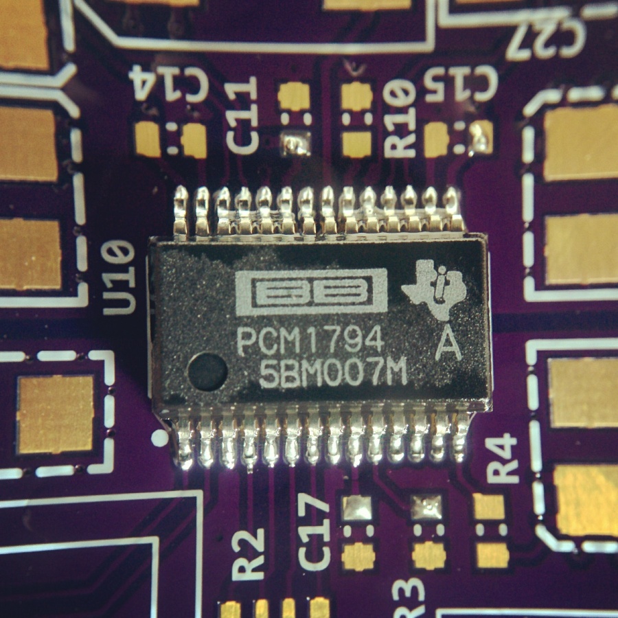
Since ODAC (rev. B) uses PCM5102A, I first went through the TI/BB catalog. The part I picked in the end is PCM1794A: 24 bit / 192 kHz, differential current output. While it's expensive ($13.83 each from Digikey), the THD+N and SNR numbers both look awesome. Its close cousin PCM1793 has integrated I/V but slightly less impressive analog performance numbers.
AK4490 remains an attractive alternative due to its popularity.
EDIT: PCM1794A has a less expensive, pin-to-pin-compatible drop-in replacement part, PCM1798.
Op-Amp
I picked OPA1612, a general-purpose dual audio op-amp. Similar to the DAC, it's expensive but the numbers are hard to beat. While it's probably overkill, it is my hope that the op-amp is "ideal enough" and therefore does not become the bottleneck of overall system analog performance.
EDIT: OPA1612 has a less expensive drop-in replacement part, OPA1662. Interestingly OPA161x offers single and dual packages, while OPA166x offers dual and quad packages.
Output
I originally wanted to use OPA1622, but it's only available in DFN package. For now I am going to simply duct tape the POT-HPF-output stages of O2 (NJM4556, 2x in parallel) and call it a day.
Schematic Design
DAC
The digital side of PCM1794A is very straightforward to hook up — just follow the datasheet. All options are pin-controlled, so for debugging I placed a 4-pack DIP switch.
The analog side is more trouble. There are two current output pins per channel: IOUT- and IOUT+. They are related to the input word as follows:
| Current [mA] | -224 | 0 | 224 – 1 |
|---|---|---|---|
| IOUT- | 2.3 | 6.2 | 10.1 |
| IOUT+ | 10.1 | 6.2 | 2.3 |
Basically they output 6.2 ± 3.9 mA. While datasheet marked negative signs in front of all these numbers, the actual direction of current flow is out of the DAC — in other words the DAC sources current. It tricked me at first and screwed my 1st version.
As mentioned before, this differential current output needs to be converted to a voltage signal first…
I/V conversion
Wikipedia: https://en.wikipedia.org/wiki/Transimpedance_amplifier

This work is licensed under the Creative Commons Attribution-ShareAlike 3.0 License. Link to original work.
(Ignore the photodiode — any current source would be the same). Current in, voltage out. V = -I*R. Very simple… So why not just use a sense resistor, like what you would do with 4-20 mA current loops? The short answer: The op-amp solution presents a constant 0V virtual ground to the current source, while the voltage drop on the sense resistor (which is the voltage output signal) is visible to the current source, which is bad.
There is a problem though: Because the current output from DAC is [2.3, 10.1] mA, the voltage output will be [-10.1*R, -2.3*R] mV, which is entirely negative. Now we need a negative power supply for the op-amp. Well, we need one for the final ground-referenced bipolar output to the headphones anyway, but since the op-amp is connected to both the positive and negative power supplies, we’re essentially wasting more than half of its output voltage swing!
While it is totally possible to “subtract” that 6.2 mA common mode current using a constant current sink, I decided not to bother with this in my first prototypes. I might mess with this idea again once I get the whole system working.
Analog Signal Processing
I have to admit that the design space is huge here. The fact that this stage sits in the middle of the signal chain does not help, as it has to match both the upstream DAC analog output and the downstream headphone driver. I figured out that it’s easier to reason from the output side instead, since the headphone driver likely expects a single-ended, bandwidth-limited signal with large voltage swing. Therefore we must at least have:
- adequate gain
- low-pass reconstruction filter
- differential to single-ended conversion
Almost every op-amp stage can have some gain. In fact we already do — the output amplitude of the I/V stage can be adjusted by its feedback resistor value.
The main design question is the LPF. Its passband needs to be sufficiently flat: ±0.1 dB from DC to 22 kHz seems to be good enough. Stopband is a little bit trickier. The DAC is 8x oversampling with a built-in digital filter (which you can disable and instead supply your own 8x up-rated data). Depending on pin configuration, you have roughly -100 dB or -20 dB at 0.6*fs, with fs being the input sample rate (i.e. output sample rate is 8*fs). Even if we choose the -20 option, we can make the first image at fstop = (8 – 0.6 = 7.4)*fs be attenuated at -40 dB by the LPF. Use fs = 96 kHz, and we have fstop = 710 kHz. Plug these into an analog filter designer and we see that we need at least 2nd order Butterworth to do the job.
Next we go with the implementation of the filter. Since we also need to do the differential to single-ended conversion, we can take the popular approach of merging it with a inverting filter topology — which in this case means a multiple feedback (MFB) design:

Sidenote: This is the same schematics in my previous post. Actually my DACPort arrived months after I tested this circuit!
The I/V section can be rigged with an additional real pole (RC stage) by connecting a capacitor in parallel with the gain resistor (which is supposed to be there for the stability of the op-amp anyway). This makes a 3rd order filter which has a even sharper roll-off. Sounds great! (pun not intended)
Simulation

https://www.partsim.com/simulator#66922 (current sources as DAC)
Didn’t I already say it’s simple?
Results:


Didn’t figure out how to export cursor data for the plots, but bode plot suggests that the filter matches specifications (using ideal components): passband -0.1 dB at 22 kHz, stopband -40 dB at 700 kHz.
Implementation
I use OSHPark for prototyping PCBs. I decided to use their 4-layer FR-408 stackup simply for an un-broken ground layer. Turns out that the analog signals can easily fit on the top layer, so I allocated the power layer to the negative rail, and the bottom layer to positive rails.
While the analog stages are very straightforward to implement, I introduced a major twist from similar designs by using exclusively 4-pack and 8-pack precision matched resistors for gains. These resistors are not available in traditional E-series values; instead they offer common integer ratios (e.g. 1:1, 1:2, 1:5, 1:9, 1:10, etc) from powers of 10. While they offer the standard 0.1% accuracy of value, the accuracy of ratio between resistors in the same package can go down to 0.05%. The 4-pack also takes 3/4 of the board space required for individual 0603 resistors, while being easier to solder by hand.
This ended up in v3.0, where I managed to pack the entire DAC-Filter module into a 2000 x 800 mil^2 rectangle, complete with distributed 10 μF bulk decoupling tantalum caps but lacking I/O connectors. The top layer (which contains all pads and signal traces) now looks like this:
NOTE: PCB artwork license: CC by-nc-sa

Note: color coded nets:
- indigo: differential audio
- green: single-ended audio
- red: all other nets
Test


PCB v1.0 returned and I soldered 2 copies: one with filter and one without. I decided to run a simple, no-stress test: make it generate a sine wave.
Sidenote: Leadless is a PITA. If iron temperature is too high, solder oxidizes fast and blackens the tip; if too low, solder won’t just flow despite generous amount of flux I squeezed onto the board. Still I somehow managed to succeed on first attempt…
I2S source
I tried to use my BeagleBone Black to generate I2S, but setting up the device tree and drivers to get what I want was so tedious I eventually gave up. Instead, I quickly wrote a simple program to run on my STM32F4 discovery board that blasts a 480 Hz sine wave through I2S (integer multiple of fs = 48 kHz so that I can simply loop over a const table). Since the master clock can go to 256*fs = 12.288 MHz, which is much higher than what I usually run SPI at, I felt I need to at least use my oscilloscope to probe the master clock input pin at DAC:

While symmetry leaves a lot to be desired, ringing seems acceptable. As this is a clock derived from STM32F4’s built-in PLL, I don’t have high hopes for jitter or accuracy. After checking serial data with my logic analyzer, I decided that it’s good enough for the time being.
Result
First I probed the output of I/V stage.

Yes, it does output a sine wave with negative DC bias. You might wonder why it is so noisy. Actually, the spurs you see on the waveform is mostly not noise. If you zoom in onto a single period:

Hmm. What is this “pixelized” look? Keep zooming in…

Here you can see the individual “steps” produced by the DAC, which themselves are sigma-delta modulated. Well, that is exactly why we need a filter! Although I initially picked a much higher cutoff frequency, you can still see that the filter output waveform is much cleaner and free of “steps”:

Summary
The DAC + Filter module works! It produces reasonably clean line-level audio signal as expected.
The immediate next module on the list is the Power Amp, which allows us to plug in an actual headphone. Combine these two with a USB-I2S bridge and we would arrive at a minimal working system from USB to headphone output. More on that in the next post.

Pingback: Making Myself a USB DAC + Headphone Amp — Part 2 – Frog in the Well
Well done!
LikeLike
Pingback: Making a USB DAC and Headphone Amp – OSH Park
Pingback: Making Myself a USB DAC + Headphone Amp — USB Interface – Frog in the Well
Pingback: Making Myself a USB DAC + Headphone Amp — Single-inductor DC-DC, Conclusion – Frog in the Well
heyy,
This is so handy. I’m trying to make a DAC myself. Can you send me to whole PCB design?
That would help me a lot.
Thanks you so much
LikeLike
Dear Summivox,
I’m a student learning electronics, I am a intern in a company what is specialized in making pcb’s for the next 5 weeks. When I make a design of the PCB they can make the PCB for me. I’m new in the electronica world so it’s impossible to design the DAC myself.
I hope you can help me out.
I adhere to the PCB artwork license Rules.
Thank you so much.
Greetings,
Mike opheij
LikeLike
hey,
I’m very intressted in your project and want to build one myself. I’m not so good with electronic’s yet (because i’m still a student :). I have read your flog all the way and make notes about it. I wonder if the files on the site hackaday.io are complete? when i sent those gerber files to a PCB company will i get al the pcb’s i need for this project or are there files and schematics missing?
except for the Amplefier because I read that you can’t share those information and i understand that. But that is no problem because that’s the only part i know to make by myself.
I hope you can help me out. i would appreciate that very much. hopefully i get a quicke respons. 🙂
greetings!!
LikeLike